Friday, 4 November 2005 - 2:12 PM
609e
Non-Lithographic Micropatterning of Thin Crystal Film Layers and Bulk Micro-Machining Via Hydrogel Stamping
Stoyan K. Smoukov, Christopher J. Campbell, Kyle J.M. Bishop, and Bartosz A. Grzybowski. Dept of Chemical and Biological Engineering, Northwestern University, 2145 Sheridan Rd/TechE136, Evanston, IL 60208
ASOMIC and the more general WETS method overcome many limitations of soft-lithographic techniques, e.g. reagents can penetrate into and modify the bulk of the substrate. Control over reaction geometries and fluxes allows patterning on the micrometer and even hundreds of nanometers scales to produce diffraction gratings, optical elements and microfluidic devices.
Several applications in deep etching of materials, doping and reactive patterning will be discussed in detail. 1-step etching of functional device prototypes is will also be highlighted.
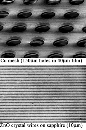
Picture: Top: an SEM image of a 40 µm Cu film etched through to give a metal membrane/sieve structure. 3D reliefs are possible with multiple stamping. The same technique can also cut out micro-objects from the foil like a cookie-cutter. Bottom: SEM of 140 nm thick, 10 µm wide ZnO wires (piezoelectric material), etched in a single 30-second step.
See more of #609 - Reactor Design and Analysis for Electronic Materials (08E10)
See more of Materials Engineering and Sciences Division
See more of The 2005 Annual Meeting (Cincinnati, OH)