
 Google
 Yelp
 Facebook
 Twitter
 ChEnected
339053 Fabrication of 3D Electrodes for Electrorotation Experiments
Fabrication of 3D Electrodes for Electrorotation Experiments
Samuel Kilchenmann* and Carlotta Guiducci*
*École Polytechnique Fédérale de Lausanne, SWITZERLAND
Introduction
Electrorotation (ROT) is a powerful technique that has been used to characterize and differentiate different particles through the extraction of their electrical parameters. Through the study of a particle's response to an electric field at specific frequencies, it is possible to extract information such as the membrane integrity of biological particles. In order to achieve high accuracy of the extracted parameters, a rotating electric field with high linearity needs to be generated. For this purpose, Goater et al. introduced bone-shaped electrodes [1]. Most devices used for electrorotation consist of planar electrodes that result in electrical fields in z-direction, which causes out of focus movements and makes trapping and observation of the particles difficult. Different groups tried to overcome this problem by designing chips with octopole cages that trap and rotate cells at the same time [2] or by combining the ROT devices with laser tweezers for trapping [3]. We introduce a novel fabrication process for three-dimensional microelectrodes that can be used for electrorotation experiments. The advantages of our design are that the generated electric field does not have any z-component and thus no out-of-focal-plane movements are exerted on the particle. Moreover, the electrodes serve as a kind of mechanical trap for the particles. Further advantages of the presented fabrication process are that the microfluidic structures can be aligned with photolithographic precision and that it is possible to work with bulky and short-working distance lenses.
Simulation
The electrical fields that are generated by 3D and planar electrodes were simulated using Comsol Multiphysics. In both cases a bone shaped design of the electrodes was used for simulation. From the top views in Fig. 1 it can be seen that both designs lead to highly linear fields in the x-y plane, however, in the case of the planar electrodes the generated field lines have components in z-direction as well. A further advantage of 3D electrodes is that local heating effects can be reduced by about an order of magnitude, while keeping in the center the same field strengths as with the planar electrodes. This is due to the higher electrode surface that is used to apply the potential, which leads to a reduction of the current density.
Microfabrication
The microfabrication process is shown in Figure 2. We start with a silicon wafer passivated by Si3N4 and SiO2 layers with thicknesses of 200 nm each. First, a photoresist is applied by spin coating and is structured by photolithography. The oxide and the nitride layers are etched and the design is transferred 300 μm deep into the silicon by a Bosch process. Then, a 10 μm thick SU-8 layer is patterned by photolithography. For better adhesion of the metal on the SU-8, the resist is hardbaked at 135°C and plasma activation is done before sputtering a Ti/Pt layer onto the structures. Afterwards, a dry film resist is laminated on the wafer and patterned by photolithography. The resist serves as etch mask for plasma etching of the metal layer. After stripping of the photoresist, a second SU-8 layer to pattern the microfluidic channels is applied. To planarize the SU-8 layer that is spun onto the high topographic surface, chemical mechanical polishing (CMP) is performed after the post exposure bake and before the development of the resist. This strategy is chosen that the undeveloped resist protects the access pads during CMP. Afterwards, the SU-8 is developed and the microfluidic accesses are opened up by etching the backside oxide and nitride layers and by grinding the wafer down to 300 μm from the backside. Finally, the wafer is diced and a coverslip is bonded onto the chips, where the SU-8 serves as adhesive. In Figure 3 we show a picture of such an electrorotation chip (a) and SEM images of (b) the 3D electrodes without glass coverage of the microfluidic channels and (c) the cross section of the whole chip with glass coverage.
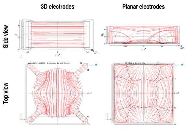
Figure 1 Comsol simulations of the electric field for planar and 3D electrodes
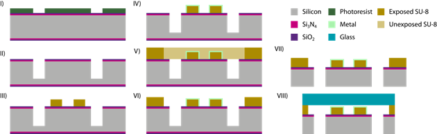
Figure 2 Fabrication process of the electrorotation chips with 3D electrodes
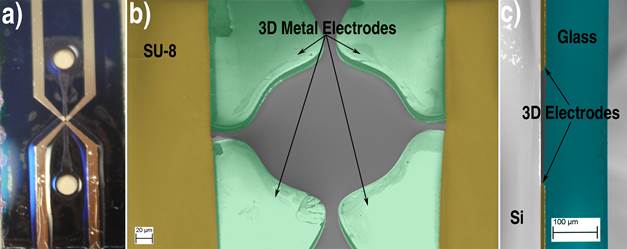
Figure 3: (a) Electrorotation chip ; (b)SEM of the 3D metal electrodes; (c)SEM of the cross-section of a chip with the glass coverage.
See more of this Group/Topical: 2013 Annual Meeting of the American Electrophoresis Society (AES)